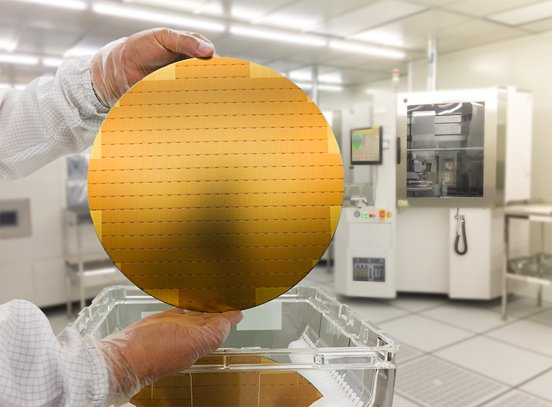
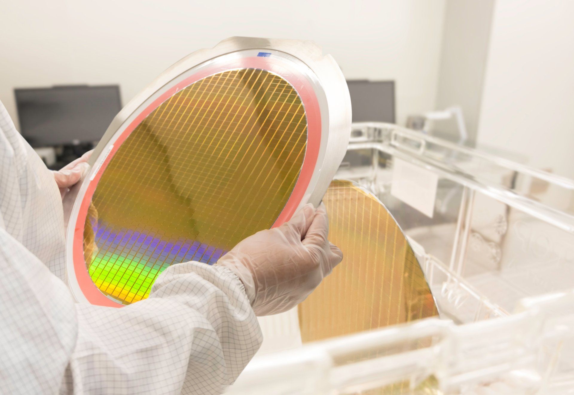
Wafer Lamination 

Wafer lamination is a critical process in semiconductor manufacturing that ensures the protection and integrity of wafers as they undergo various stages of production. At GTI Technologies, we understand that wafer lamination entails the application of a laminating film over the wafer's surface to create a barrier that guards against contaminants, mechanical stress, and other environmental factors that could compromise the wafer's quality. Proper wafer lamination is essential for maintaining the uniformity of the wafer throughout the manufacturing process, which in turn is crucial for the functionality and reliability of the semiconductor devices.

CALL US TODAY
Over 45 years of experience
All over North America and Europe
Delivering and supporting machines

How to Achieve Precision and Uniformity with Wafer Lamination


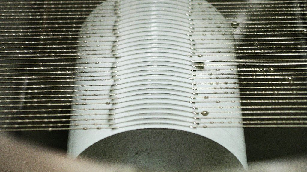
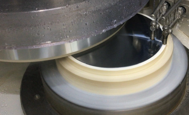
Achieving precision and uniformity with wafer lamination requires working with our state-of-the-art supplier of manufacturing equipment. Our film laminator is designed for delicate handling and application. Such equipment ensures that the semiconductor equipment used in the lamination process adheres to strict industry standards. On the other hand, vacuum lamination is particularly effective in creating a bubble-free and uniform layer, which is vital for the success of further processing steps such as photolithography and etching. Advanced film laminator systems are utilized for precision control, allowing for exact film tension and placement. Additionally, using high-quality backgrind and tape lamination materials further enhances the wafer's stability and readiness for subsequent fabrication phases.

A person in a cleanroom suit and gloves is handling a silicon wafer with a shiny, reflective surface. The wafer is held over a transparent container, with another wafer inside. Computer monitors are visible in the background.

Our Process

01.

Work together with our customers and suppliers to clearly understand the application and our customer’s needs and potential solutions. 

02.

Test our preferred solution, evaluate with the customer. 

03.

Present and then deliver solutions on-time. 

04.

Support our customers with training, spare parts, and ongoing engineering resources. 

MORE ABOUT US

Discover Our Advanced Wafer Lamination


Explore our comprehensive wafer lamination solutions and discover how our advanced techniques can benefit your semiconductor equipment manufacturing process. Our expertise in wafer lamination ensures that your wafers are laminated with the utmost precision, providing a consistent and protective layer necessary for high-quality device production. For more information about our wafer lamination techniques and services, navigate our about us page. If you want to use our sophisticated wafer lamination services or have any questions, contact us today. Our team is dedicated to supporting your operations with superior wafer lamination solutions that drive productivity, enhance quality, and meet the needs of even the most stringent semiconductor applications.

CALL US TODAY
November 8, 2024
Visit GTI at SEMICON EUROPA, NOV 2024
November 8, 2024
Visit GTI at ECTC, May 2025
December 18, 2018
Wire sawing, whether using abrasive slurry or diamond wire, offers distinct advantages over other cutting methods in many applications. The high precision, reduced kerf loss, and reduced damage of wire sawing can have a substantial effect not only on the cutting process, but also on downstream operations. REDUCED KERF LOSS: The first advantage of wire sawing is reduced kerf loss (the material lost during cutting). Compared with ID saws (0.300 to 0.500mm kerf) and diamond blade saws (0.200 to 3.00mm), a multi wire saw can produce kerfs of less than 0.200mm with slurry, and 0.15 to 0.26mm with diamond wire. This material savings add up; after spending substantial time and money growing a perfect crystal or other material, reducing kerf loss helps save precious material and increase yields. REDUCED DAMAGE: Wire sawing is a relatively gentle process, particularly when cutting with slurry. The gentle, low-force cutting action and fine abrasive leads to reduced depth of damage on the cut surface. This reduction in sub-surface damage means less stress in the material and less material that needs to be ground, lapped, or polished after slicing. Once again this saves material, and reducing the amount of removal necessary after slicing means a customer can cut thinner pieces, further improving yields and lowering cost. The reduced damage also extends to the entry and exit points of the cut – the gentle cutting action means less chipping or other physical damage, leaving clean corners and improving quality. Even cutting with diamond wire, a more aggressive process than slurry, is quite gentle relative to other cutting methods, so many of the same benefits apply. BETTER GEOMETRY : A goal of any cutting method is to create flat, consistent pieces, and here a wire saw excels. TTV, bow, and warp are all minimized. This again reduces the need for post-processing, improving yields. HIGHER THROUGHPUT: On the surface, wire sawing is slow. The trade off of such a gentle cutting method is that the machine moves through the workpiece slowly, so cycle times are long. Despite this, wire sawing is actually very efficient due to the use of multiple wires. A production machine can have hundreds of wires contacting the workpiece simultaneously. As a result, at the end of a single cutting cycle the entire length of material will be completed. On particularly hard materials, using diamond wire can significantly improve throughput, though it can also raise the cost per slice. We examine each application to find the most efficient process. Wire sawing is an excellent solution to many of the challenges facing companies looking to produce wafers and other thin pieces from delicate, valuable, and very hard materials. It is the best solution for slicing silicon carbide, sapphire, GaN, glass, ceramics, and more. Contact GTI today to learn how wire sawing can work for your application.

Contact us


Hours

Monday - Friday: 8AM-5PM


Service Area

6 Armstrong Road,

Shelton, CT 06484, USA


Phone


European Contact

JTA Equipment Technology

+44 7906 388 508

jta-ltd.com


Share by: