permanent bonding
Permanent bonding plays a critical role in the fabrication process of semiconductor devices, providing the stability and durability needed for components that are meant to last. At GTI Technologies, we understand that this procedure is closely associated with the creation of microelectromechanical systems (MEMS) and advanced integrated circuits where layers of different substrates need to be joined with enduring strength. As technology continues to miniaturize and require more complex assemblies, the demand for high-quality permanent bonding solutions has never been higher. Our state-of-the-art bonding techniques ensure an impeccable bond integrity that meets the rigorous standards of the semiconductor industry.
Wafer Bonding or Permanent Bonding — What Do You Need?
Wafer bonding is a pivotal step that enables vacuum bonding processes, which are crucial for intricate tasks such as layer transfer or thin wafer handling. Regarding semiconductor manufacturing, the choice between temporary and permanent bonding depends on the specific application and process requirements. As a renowned supplier of manufacturing equipment, our solutions include a variety of equipment designed to cater to both temporary and permanent bonding needs with exceptional precision.
Wafer Bonding Using Double-Sided Tape
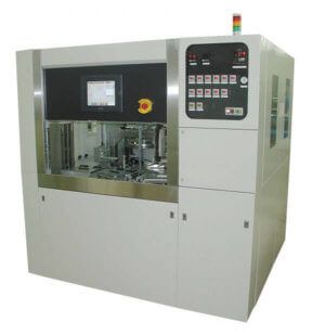
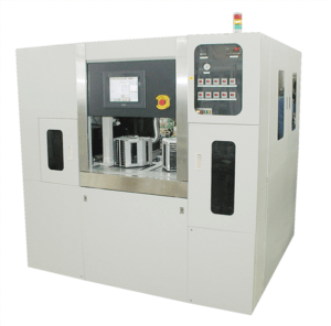
In the realm of semiconductor equipment, we provide reliable temporary bonding materials. They protect the wafer during thinning and grinding operations. Furthermore, our extensive experience with permanent bonding technology ensures robust and lasting connections for devices that require long-term performance. Examples of the machines we provide include:
| Machine | Wafer size | Throughput | Machine size (WxDxH) |
|---|---|---|---|
| GWS-300 | Up to 300mm | Up to 40wph | 2,400x2,400x1,800mm |
| GWSM-300M | Up to 300mm | Up to 30wph | 700x1,200x1,600mm |
| WSM-100 | Up to 200mm | Up to 40wph | 1,700x1,760x1,800mm |
| WSM-200 | Up to 200mm | Up to 40wph | 1,800x1,800x1,800mm |
- GWS-300 — GWS is a fully automated solution for bonding wafers up to 300mm. Wafers are presented to the tool with adhesive already applied, and then they are bonded in a vacuum chamber for maximum quality.
- GWSM-300M - Manually loaded version of GWS-300. Bond wafers up to 300mm in a vacuum chamber.
- WSM-100 - This machine is Takatori’s solution for temporarily bonding wafers up to 200mm using double-sided tape. Choose heat-release or UV-release double-sided tape to bond wafers quickly and cost-effectively. Vacuum bonding occurs in a vacuum chamber to ensure the highest quality and eliminate bubbles.
- WSM-200 - This machine is a bonding and mounting solution for wafers up to 200mm. It first mounts wafers on a dicing frame using Takatori’s vacuum bonding technology and then removes the carrier wafer using either heat or UV exposure (depending on the backgrind tape/adhesive type used).
Explore Our Precision Techniques
Our company sets the industry standard for those seeking the utmost precision in permanent bonding techniques. Whether your project requires the flexibility of temporary bonding or the robustness of permanent bonding, our expertise is at your disposal. We're committed to helping you find the perfect bonding solution that aligns with your production goals. If you’re ready to enhance your semiconductor fabrication process with advanced bonding technology, please feel free to contact us. Our team is dedicated to providing comprehensive support and tailored solutions, ensuring that you receive the best possible outcome for your bonding requirements.


