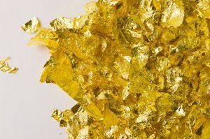
Many semiconductor devices particularly those made with gallium arsenide (GaAs) or indium phosphide (InP), require the removal of metal layers by etching. Gold, for example, difficult and expensive to remove by etching due to its inertness. Lift off provides an alternative to etching. A pattern is first created in a sacrificial layer of photoresist before the gold is the deposited. The gold adheres strongly to the underlying device layers of GaAs (or deposited insulating layers,) and also to the photoresist which does not adhere as strongly to the device layers.
Standard lift-off processes use solvents to remove the resist, and often take the gold with it. The main problems with this process are:
- redeposition of the gold from the solution onto the wafer,
- disposal of the solvent is expensive, and
- reclaiming the gold from the solvent is not easy and it is too costly to throw away.
Takatori’s AMR-2200G system provides an effective alternative that does not use solvents! The system applies an adhesive tape to the wafer surface and then lifts it off in a controlled manner designed to match the specific device requirements. The gold on the photoresist is removed with the resist, while the gold adhered to the underlying device layers remains on the wafer surface undisturbed.
Benefits of this lift off with tape are:
- eliminates potential for gold being redeposited on the wafer surface,
- lowers overall cost since no solvent disposal is need, and
- makes it easy to reclaim the gold from the roll of tape.
This process is used successfully by many GaAs device fabricators. It can be used with many different metals; including gold, indium, and aluminum.
Contact GTI today to learn more about Takatori’s tape-based liftoff solution and how it can improve your bottom line.